
Revolutionizing the World through Cutting-Edge Technology and Connectivity
The semiconductor industry includes the design and fabrication of semiconductors and semiconductor devices, such as transistors and integrated circuits.
The fabrication process normally divided into several steps, Wafer fabrication, frontend process, and backend process. It is highly sophisticated and the requirement if very stringent every step throughout the manufacturing processes.

Advanced Imaging Equipment
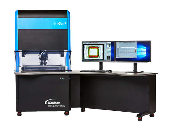
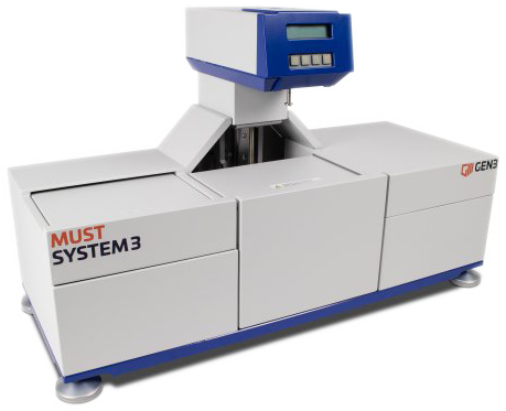
Detect flaws and defects in objects (e.g. samples) through ultrasound
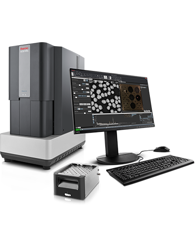
A desktop version of the electron microscope, equipped with a simplified user interface and design as compared to the electron microscope.
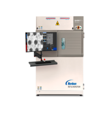
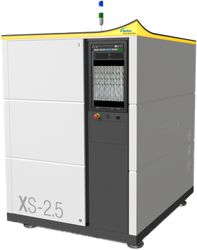
Detect flaws and defects in objects (e.g. samples) through X-rays.
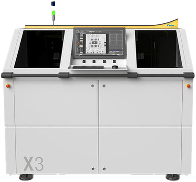
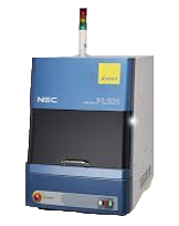
The X-platform series is a dedicated high speed inline automated X-ray inspection system for the inspection of PCB-assembly boards for single/multipanels or samples in trays. The system offers market leading inspection speed and is ideal for low-mix high-volume production environment.
An automated version of X-ray inspection equipment with enhanced process automation features, including automated anomaly detection function.
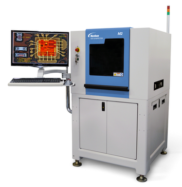
State-of-the-art automated optical, microelectronics, conformal coat and solder paste inspection systems provide our customers with fast, accurate inspection they can count on.
Optical & Portable Equipment
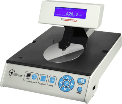
Provide measurement of thickness and bow of all wafer materials including Silicon, Gallium-Arsenide, Indium-Phosphide and sapphire or tape
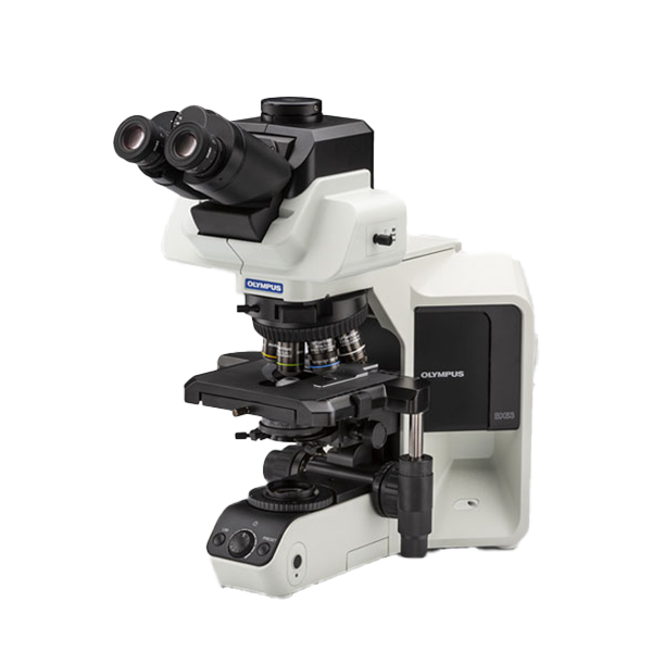
An optical instrument that uses a combination of lenses to produce magnified image for quality inspection and analysis of samples.
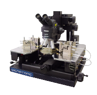
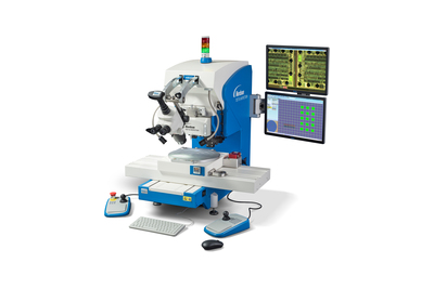
To position electrical or radio frequency (RF) probes onto a sample to test its response to external stimulus.
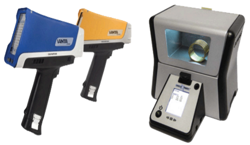
To perform elemental analysis on samples through X-ray fluorescence.
Coating Thickness, Elemental Analysis & RoHS Inspection Using X-Ray Fluorescence Analyzer.
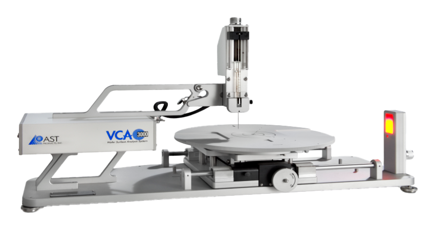
Wafer Surface Analysis Systems are specially designed for use in wafer processing quality control that provides quick and accurate contact angle/surface energy analysis on wafer surface to evaluate adhesion, cleanliness and coatings.
Advanced Analytical & Testing Equipment
Accurate and comprehensively equipped test system capable of measuring down to 0.001mN.
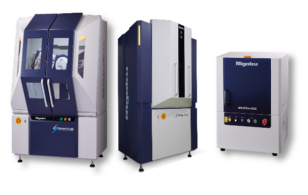
To analyse physical properties such as phase composition, crystal structures and orientation of powder, solid and liquid samples through X-ray diffraction.
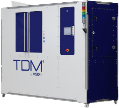
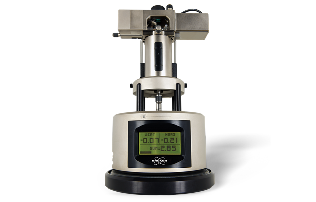
State of the art deformation or warpage measurement system for devices under thermal stress evaluation ideal for research development, quality and reliability, process development, and failure analysis studies.
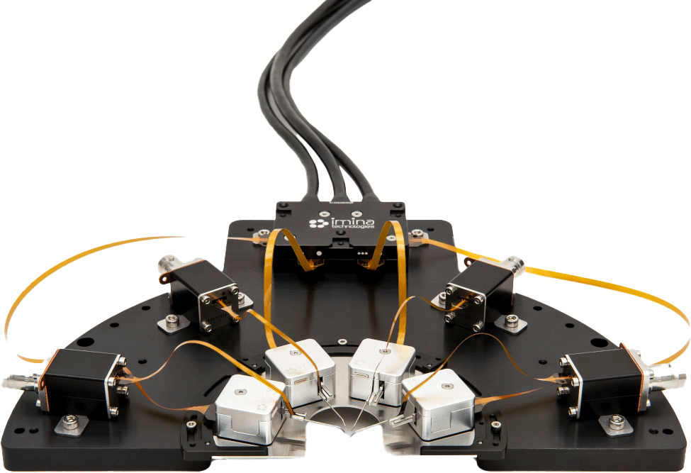
Microprobing solutions for optical microscopes, probe stations and inspection tools. Precisely position probes and physically interact with your samples even in the most confined environments.
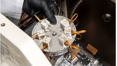
To perform electrical characterisation of microelectronic devices, in situ semiconductor failure analysis and manipulation of single structures under an electron, ion and/or optical microscopes.
To conduct destructive testing, wherein a sample is tested beyond its designed tolerance level in an attempt to analyse the integrity of the sample against physical force (e.g. pulling, pressing, and shearing).
To obtain high-resolution images to measure and visualise materials at an atomic and nano scale.
Sample Management Equipment
To remove the moulding compound of E&E components to expose the integrated circuit ("IC") chips and dies within, which then allows users to inspect and identify any defects in the IC chips and dies.
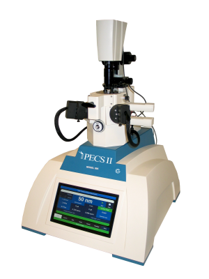
Broad argon ion beam system designed to polish and coat samples for SEM imaging and analytical techniques.
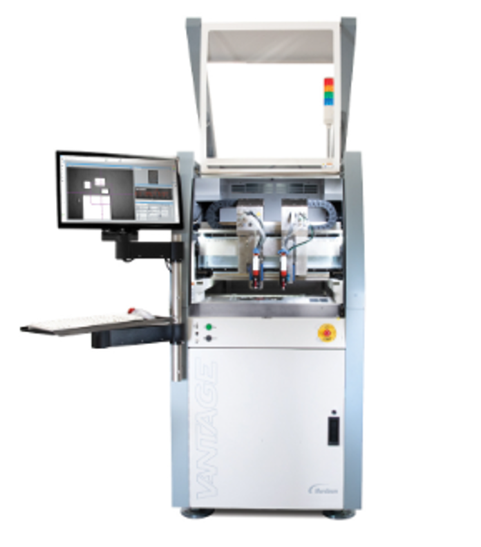
To precisely and consistently dispense the required amount of fluids into the micron-sized gaps present between IC chips and components on the printed circuit board, thereby facilitating electrical interconnect, providing structural integrity and ensuring optimal heat transfer for reliable performance.
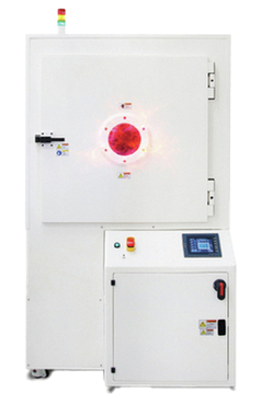
Plasma treatment systems suit various plasma cleaning, surface activation, and adhesion improvement applications. The systems deliver exceptionally uniform plasma cleaning and treatment.
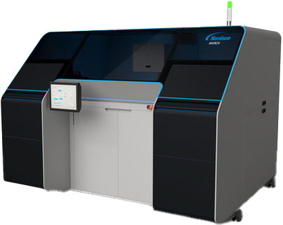
Plasma treatment systems offer high-throughput, strip-type, and inline boat processing for advanced semiconductor packaging applications.
Please complete the form and you will be contacted shortly.